Hostname: page-component-586b7cd67f-t8hqh Total loading time: 0 Render date: 2024-11-23T11:25:37.306Z Has data issue: false hasContentIssue false

Imaging Atomically Thin Transition Metal Dichalcogenides Using Deep Ultraviolet Photoelectron Emission Microscopy

Published online by Cambridge University Press:  22 July 2022

Alex M. Boehm
Affiliation:
Sandia National Laboratories, Albuquerque, New Mexico, United States
Morgann Berg
Affiliation:
Sandia National Laboratories, Albuquerque, New Mexico, United States
Cherrelle J. Thomas
Affiliation:
Sandia National Laboratories, Albuquerque, New Mexico, United States
Fangze Liu
Affiliation:
Los Alamos National Laboratory, Los Alamos, New Mexico, United States
Sean Smith
Affiliation:
Sandia National Laboratories, Albuquerque, New Mexico, United States
Calvin K. Chan
Affiliation:
Center for National Security Initiatives, University of Colorado Boulder, Boulder, Colorado, United States
Aditya D. Mohite
Affiliation:
Department of Chemical and Biomolecular Engineering, Rice University, Houston, Texas, United States
Thomas E. Beechem
Affiliation:
School of Mechanical Engineering, Purdue University, West Lafayette, Indiana, United States
J. J. Fonseca
Affiliation:
Jacobs Technology Contractor at the U.S. Naval Research Laboratory, Washington, District of Columbia, United States
C. D. Spataru
Affiliation:
Sandia National Laboratories, Livermore, California, United States
J. T. Robinson
Affiliation:
U.S. Naval Research Laboratory, Washington, District of Columbia, United States
Taisuke Ohta*
Affiliation:
Sandia National Laboratories, Albuquerque, New Mexico, United States
*
*Corresponding author: [email protected]

Abstract

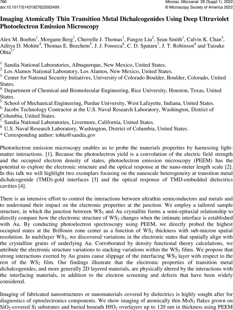
Image of the first page of this content. For PDF version, please use the ‘Save PDF’ preceeding this image.'
Type
Science of Metrology with Electrons
Copyright
Copyright © Microscopy Society of America 2022

References

Hüfner, S in “Photoelectron Spectroscopy, Principles and Applications”, (Springer, Berlin) p. 347.Google Scholar
Bauer, E in “Surface Microscopy with Low Energy Electrons”, (Springer, New York) p. 25.Google Scholar
Thomas, C J, Fonseca, J J, Spataru, C D, Robinson, J T, Ohta, T, ACS Nano, 15 (2021), p. 18060. doi:10.1021/acsnano.1c06676CrossRefGoogle Scholar
Berg, M, Liu, F, Smith, S, Copeland, R G, Chan, C K, Mohite, A D, Beechem, T E, Ohta, T, Phys. Rev. Applied, 12 (2019), p. 064064. doi:10.1103/PhysRevApplied.12.064064CrossRefGoogle Scholar
We acknowledge insightful discussions with N. Bartelt, M. B. Sinclair, and W. T. S. Luk. We thank G. Copeland for his assistance in the PEEM measurement. The work at Sandia National Laboratories was supported by Sandia's LDRD program and the Center for Integrated Nanotechnologies user program, an Office of Science User Facility operated for the U.S. Department of Energy (DOE) Office of Science (DEAC04-94AL85000). The work at the U.S. Naval Research Laboratory (NRL) was funded by the Office of Naval Research. Sandia National Laboratories is a multimission laboratory managed and operated by National Technology and Engineering Solutions of Sandia, LLC., a wholly owned subsidiary of Honeywell International, Inc., for the U.S. Department of Energy's National Nuclear Security Administration under contract DE-NA0003525. The views expressed in the article do not necessarily represent the views of the U.S. Department of Energy or the United States Government.Google Scholar