Hostname: page-component-586b7cd67f-rdxmf Total loading time: 0 Render date: 2024-11-27T04:51:47.144Z Has data issue: false hasContentIssue false

e-Beam Detection of Buried Open Defects in Semiconductor Device

Published online by Cambridge University Press:  05 August 2019

Kwame Owusu-Boahen
Affiliation:
Samsung Austin Semiconductor, LLC, Austin, TX, USA.
Po-Chin Kuo
Affiliation:
Samsung Austin Semiconductor, LLC, Austin, TX, USA.
Thaung H. Oo
Affiliation:
Samsung Austin Semiconductor, LLC, Austin, TX, USA.
Liliam E. Fernandez
Affiliation:
Samsung Austin Semiconductor, LLC, Austin, TX, USA.
Carl Chang Hun
Affiliation:
Samsung Austin Semiconductor, LLC, Austin, TX, USA.

Abstract

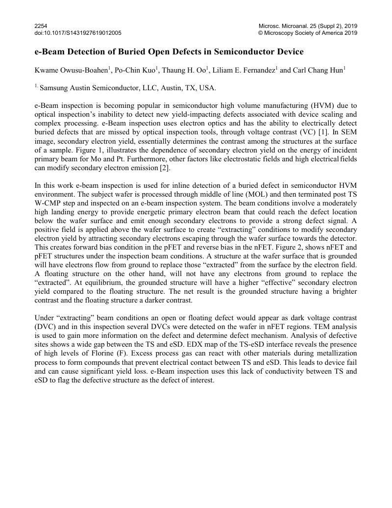
Image of the first page of this content. For PDF version, please use the ‘Save PDF’ preceeding this image.'
Type
Microscopy and Spectroscopy of Nanoscale Materials for Energy Applications
Copyright
Copyright © Microscopy Society of America 2019 

References

[1]Soucek, M et al. , Semiconductor International 26(8) (2003), p. 80.Google Scholar
[2]Yougui, L, in “Practical Electron Microscopy and Database”, (GlobalSino).Google Scholar