Hostname: page-component-586b7cd67f-dlnhk Total loading time: 0 Render date: 2024-11-29T19:10:46.895Z Has data issue: false hasContentIssue false

4D-STEM Measurement of Thickness and Orientation by Bloch Wave Dynamical Diffraction Matching

Published online by Cambridge University Press:  22 July 2022

Steven E Zeltmann*
Affiliation:
Materials Science and Engineering Department, University of California Berkeley, Berkeley, CA, USA
Andrew M Minor
Affiliation:
Materials Science and Engineering Department, University of California Berkeley, Berkeley, CA, USA National Center for Electron Microscopy, Molecular Foundry, Lawrence Berkeley National Laboratory, Berkeley, CA, USA
Colin Ophus
Affiliation:
National Center for Electron Microscopy, Molecular Foundry, Lawrence Berkeley National Laboratory, Berkeley, CA, USA
*
*Corresponding author: [email protected]

Abstract

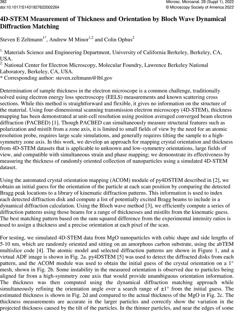
Image of the first page of this content. For PDF version, please use the ‘Save PDF’ preceeding this image.'
Type
Developments of 4D-STEM Imaging - Enabling New Materials Applications
Copyright
Copyright © Microscopy Society of America 2022

References

LeBeau, et al. , Phys Rev B 79(21), p. 214110.CrossRefGoogle Scholar
Ophus, et al. , Microscopy and Microanalysis (2021), p. 1.Google Scholar
DeGraef, in “Introduction to Conventional Transmission Electron Microscopy” (2003).Google Scholar
Madsen, and Susi, , Open Research Europe 1 (2021), p. 24.CrossRefGoogle Scholar
Savitzky, et al. , Microscopy and Microanalysis 27(4) (2021), p. 712.10.1017/S1431927621000477CrossRefGoogle Scholar
Work at the Molecular Foundry was supported by the Office of Science, Office of Basic Energy Sciences, of the U.S. Department of Energy under Contract No. DEAC02-05CH11231. SEZ was supported by the National Science Foundation under STROBE Grant No. DMR 1548924.Google Scholar