Hostname: page-component-586b7cd67f-vdxz6 Total loading time: 0 Render date: 2024-11-26T06:38:06.207Z Has data issue: false hasContentIssue false

Electrostatic charging and manipulation of semiconductor nanowires

Published online by Cambridge University Press:  23 June 2011

Vincent C. Holmberg
Affiliation:
Department of Chemical Engineering, Center for Nano and Molecular Science and Technology, Texas Materials Institute, The University of Texas at Austin, Austin, Texas 78712
Reken N. Patel
Affiliation:
Department of Chemical Engineering, Center for Nano and Molecular Science and Technology, Texas Materials Institute, The University of Texas at Austin, Austin, Texas 78712
Brian A. Korgel*
Affiliation:
Department of Chemical Engineering, Center for Nano and Molecular Science and Technology, Texas Materials Institute, The University of Texas at Austin, Austin, Texas 78712
*
a)Address all correspondence to this author. e-mail: [email protected]
Get access

Abstract

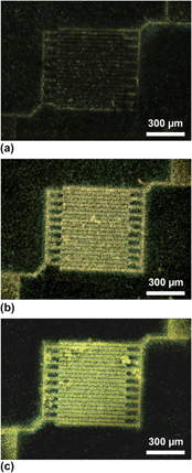
It was observed that silicon and germanium nanowires can exhibit significant electrostatic charging and respond strongly to externally applied electric fields. This includes nanowires in air and dispersed in low-conductivity, low-dielectric-constant solvents such as hexane, toluene, and benzene. The electrostatic charging of semiconductor nanowires was investigated as a tool for nanowire manipulation. By charging a substrate, nanowires could be deposited on surfaces with very high coverage and onto selected locations of the surface. The density of deposited nanowires could be adjusted systematically by varying the strength of the electric field. Alternating electric fields, applied between two electrodes, resulted in nanowires oriented with respect to the field orientation.

Type
Articles
Copyright
Copyright © Materials Research Society 2011

Access options

Get access to the full version of this content by using one of the access options below. (Log in options will check for institutional or personal access. Content may require purchase if you do not have access.)

References

REFERENCES

1.Hanrath, T. and Korgel, B.A.: Nucleation and growth of germanium nanowires seeded by organic monolayer-coated gold nanocrystals. J. Am. Chem. Soc. 124, 1424 (2002).CrossRefGoogle ScholarPubMed
2.Hanrath, T. and Korgel, B.A.: Supercritical fluid-liquid-solid (SFLS) synthesis of Si and Ge nanowires seeded by colloidal metal nanocrystals. Adv. Mater. 15, 437 (2003).CrossRefGoogle Scholar
3.Lee, D.C., Hanrath, T., and Korgel, B.A.: The role of precursor-decomposition kinetics in silicon-nanowire synthesis in organic solvents. Angew. Chem. Int. Ed. 44, 3573 (2005).CrossRefGoogle ScholarPubMed
4.Tuan, H.-Y. and Korgel, B.A.: Importance of solvent-mediated phenylsilane decomposition kinetics for high-yield solution-phase silicon nanowire synthesis. Chem. Mater. 20, 1239 (2008).CrossRefGoogle Scholar
5.Abbasi, T. and Abbasi, S.A.: Dust explosions–cases, causes, consequences, and control. J. Hazard. Mater. 140, 7 (2007).CrossRefGoogle ScholarPubMed
6.Gibson, N. and Lloyd, F.C.: Electrification of toluene flowing in large-diameter metal pipes. J. Phys. D: Appl. Phys. 3, 563 (1970).CrossRefGoogle Scholar
7.Glor, M.: Hazards and problems associated with liquids. J. Electrost. 51, 359 (2001).CrossRefGoogle Scholar
8.Holmberg, V.C. and Korgel, B.A.: Corrosion resistance of thiol- and alkene-passivated germanium nanowires. Chem. Mater. 22, 3698 (2010).CrossRefGoogle Scholar
9.Smith, D.A., Holmberg, V.C., and Korgel, B.A.: Flexible germanium nanowires: Ideal strength, room temperature plasticity, and bendable semiconductor fabric. ACS Nano 4, 2356 (2010).CrossRefGoogle ScholarPubMed
10.Yuan, J., Liu, X., Akbulut, O., Hu, J., Suib, S.L., Kong, J., and Stellacci, F.: Superwetting nanowire membranes for selective absorption. Nat. Nanotechnol. 3, 332 (2008).CrossRefGoogle ScholarPubMed
11.Holmberg, V.C., Rasch, M.R., and Korgel, B.A.: PEGylation of carboxylic acid-functionalized germanium nanowires. Langmuir 26, 14241 (2010).CrossRefGoogle ScholarPubMed
12.Charged Ge Nanowire Fabric (mp4) is a video of the electrostatic charging phenomena shown in Fig. 2. It is available online at http://journals.cambridge.org/jmr.Google Scholar
13.Electrostatic Repulsion (mp4) is a video of Si nanowires in toluene moving in response to the static charge on a nitrile glove. It is available online at http://journals.cambridge.org/jmr.Google Scholar
14.Davies, D.K.: Charge generation on dielectric surfaces. J. Phys. D: Appl. Phys. 2, 1533 (1969).CrossRefGoogle Scholar
15.Pierce, D.S.: Mechanics of Impression Evidence (CRC Press, London, England, 2011), p. 191.CrossRefGoogle Scholar
16.Protasenko, V., Gordeyev, S., and Kuno, M.: Spatial and intensity modulation of nanowire emission induced by mobile charges. J. Am. Chem. Soc. 129, 13160 (2007).CrossRefGoogle ScholarPubMed
17.Zhou, R., Chang, H-C., Protasenko, V., Kuno, M., Singh, A.K., Jena, D., and Xing, H.: CdSe nanowires with illumination-enhanced conductivity: Induced dipoles, dielectrophoretic assembly, and field-sensitive emission. J. Appl. Phys. 101, 073704 (2007).CrossRefGoogle Scholar

Holmberg supplementary movies

Movie 1

Download Holmberg supplementary movies(Video)
Video 431 KB

Holmberg supplementary movies

Movie 2

Download Holmberg supplementary movies(Video)
Video 580.9 KB