Hostname: page-component-745bb68f8f-grxwn Total loading time: 0 Render date: 2025-01-11T06:33:54.408Z Has data issue: false hasContentIssue false

A Q-DLTS investigation of aluminum nitride surface termination

Published online by Cambridge University Press:  13 March 2012
Jason B. Rothenberger*
Affiliation:
Nuclear Science and Engineering Institute, University of Missouri, Columbia, Missouri 65211
Daniel E. Montenegro
Affiliation:
Nuclear Science and Engineering Institute, University of Missouri, Columbia, Missouri 65211
Mark A. Prelas
Affiliation:
Nuclear Science and Engineering Institute, University of Missouri, Columbia, Missouri 65211
Tushar K. Ghosh
Affiliation:
Nuclear Science and Engineering Institute, University of Missouri, Columbia, Missouri 65211
Robert V. Tompson
Affiliation:
Nuclear Science and Engineering Institute, University of Missouri, Columbia, Missouri 65211
Sudarshan K. Loyalka
Affiliation:
Nuclear Science and Engineering Institute, University of Missouri, Columbia, Missouri 65211
*
a)Address all correspondence to this author. e-mail: [email protected]
Get access

Abstract

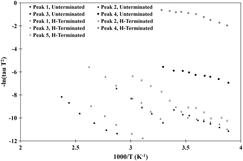
A single crystal aluminum nitride (AlN) wafer surface was investigated via the use of a novel software-based, Charge-based Deep Level Transient Spectroscopy (Q-DLTS) apparatus, both before and after surface bond termination with hydrogen plasma. The sample was cleaned and metalized with a thermoresistive evaporator to create electrical contacts and then annealed in a helium atmosphere at 825 °C. Current-voltage (I-V) measurements were performed to investigate the nature of the metal/substrate contacts. The effect of hydrogen termination was investigated and Arrhenius plots were produced from Q-DLTS spectra at temperatures ranging from −15.9 °C to 136.0 °C. Activation energies and capture cross-section values were calculated from the Q-DLTS spectra for traps existing in the AlN substrate surface. Prior to hydrogen termination, four charge traps were observed with activation energies of 0.31 eV, 0.61 eV, 0.56 eV, and 0.18 eV and capture cross sections 5.6 × 10⁻²¹ cm2, 1.1 × 10⁻¹⁶ cm2, 3.5 × 10⁻¹⁹ cm2, and 1.3 × 10⁻²¹ cm2, respectively After hydrogen termination, five charge traps were observed with activation energies of 0.31 eV, 0.61 eV, 0.52 eV, 0.19 eV, and 0.40 eV, and capture cross sections 4.9 × 10⁻²¹ cm2, 1.3 × 10⁻¹⁶ cm2, 2.9 × 10⁻¹⁹ cm2, 3.1 × 10⁻¹⁹ cm2, and 4.7 × 10⁻¹⁹ cm2, respectively. Four of these peaks after termination are matched with the peaks prior to termination and the fifth peak appears to be the result of the hydrogen termination.

Type
Articles
Copyright
Copyright © Materials Research Society 2012

Access options

Get access to the full version of this content by using one of the access options below. (Log in options will check for institutional or personal access. Content may require purchase if you do not have access.)

References

REFERENCES

1.Prelas, M.A. and Saha, K.: Wide band-gap electronic materials, in Encyclopedia of Chemical Processing, edited by Lee, S. (CRC Press, Boca Raton, FL, 2005) p. 3227.Google Scholar
2.Strite, S. and Morkoc, H.: GaN, AlN, and InN: A review. J. Vac. Sci. Technol., B 10, 1237 (1992).CrossRefGoogle Scholar
3.Harman, J., Kabulski, A., Pagan, V.R., Famouri, P., Kasarla, K.R., Rodak, L.E., Hensel, J.P., and Korakakis, D.: Effect of contact metals on the piezoelectric properties of aluminum nitride thin films. J. Vac. Sci. Technol., B 26, 1417 (2008).CrossRefGoogle Scholar
4.Yacobi, B.G.: Semiconductor Materials—An Introduction to Basic Principles (Kluwer Academic, New York, 2003) pp. 3840, 215.Google Scholar
5.Yonenaga, I., Ohno, Y., Taishi, T., and Tokumoto, Y.: Recent knowledge of strength and dislocation mobility in wide band gap semiconductors. Physica B 404, 4999 (2009).CrossRefGoogle Scholar
6.Polyakov, A.Y., Smirnov, N.B., Govorkov, A.V., Yugova, T.G., Scherbatchev, K.D., Avdeev, O.A., Chemekova, T.Y., Mokhov, E.N., Nagalyuk, S.S., Helava, H., and Makarov, Y.N.: Deep centers in bulk AlN and their relation to low-angle dislocation boundaries. Physica B 404, 4939 (2009).Google Scholar
7.Soltamov, V.A., Ilyin, I.V., Soltamova, A.A., Tolmachev, D.O., Mokhov, E.N., and Baranov, P.G.: Identification of the deep-level defects in AlN single crystals: EPR and TL studies. Diamond Relat. Mater. 20, 1085 (2011).Google Scholar
8.Chemekova, T.Y., Avdeev, O.V., Barash, I.S., Mokhov, E.N., Nagalyuk, S.S., Roenkov, A.D., Segal, A.S., Makarov, Y.N., Ramm, M.G., Davis, S., Huminic, G., and Helava, H.: Sublimation growth of 2 inch diameter bulk AlN crystals. Phys. Status Solidi C 5, 1612 (2008).Google Scholar
9.Polyakov, V.I., Rukovishnikov, A.I., Khomich, A.V., Druz, B.L., Kania, D., Hayes, A., Prelas, M.A., Tompson, R.V., Ghosh, T.K., and Loyalka, S.K.: Surface phenomena of the thin diamond-like carbon films, in Properties and Proceedings of Vapor-Deposited Coatings, edited by Johnson, R.N., Lee, W.Y., Pickering, M.A., and Sheldon, B.W. (Mater. Res. Soc. Symp. Proc. 555, Warrendale, PA, 1998) p. 345.Google Scholar
10.Prelas, M.A., Ghosh, T., Tompson, R.V., Viswanath, D., and Loyalka, S.K.: Electrostatic Thin Film Chemical and Biological Sensor, US Patent & Trademark Office (The Curators of the University of Missouri, Columbia, MO, 2007) p. 29.Google Scholar
11.Ghosh, T.K., Prelas, M.A., Viswanath, D.S., and Loyalka, S.K.: Science and Technology of Terrorism and Counterterrorism (Marcel Dekker Inc., New York, 2002) p. 608, 434.Google Scholar
12.Polyakov, V.I., Mityagin, A.Y., Rukovishnikov, A.I., Druz, B., Zaritsky, I., and Yervtukchov, Y.: Effect of various absorbates on electronic states of the thin diamond-like carbon films. Diamond Relat. Mater. 15, 1926 (2006).CrossRefGoogle Scholar
13.Polyakov, V.I., Rukovishnikov, A.I., Rossukanyi, N.M., Pereverzev, V.G., Pimenov, S.M., Carlisle, J.A., Gruen, D.M., and Loubnin, E.N.: Charge-based deep level transient spectroscopy of undoped and nitrogen-doped ultrananocrystalline diamond films. Diamond Relat. Mater. 12, 1776 (2003).Google Scholar
14.Polyakov, V.I., Rukovishnikov, A.I., and Ralchenko, V.G.: Surface Phenomena of CVD Diamond Films (Electrochem. Soc., 204th Meeting Proc., Honolulu, HI, 2004) p. 1801.Google Scholar
15.Wolkenstein, T.: Electronic Processes on Semiconductor Surfaces During Chemisorption (Plenum Publishing, New York, 1991).CrossRefGoogle Scholar
16.Volkenstein, F.F.: Electronic processes at the surface of a semiconductor during chemisorption. Sov. Phys. Usp. 9, 275 (1967).Google Scholar
17.Zant, P.V.: Microchip Fabrication, 5th ed. (McGraw Hill, New York, 2004) p. 609, 40–41.Google Scholar
18.King, S.W., Barnak, J.P., Bremser, M.D., Tracy, K.M., Ronning, C., and Davis, R.F.: Cleaning of AlN and GaN surface. J. Appl. Phys. 84, 5248 (1998).Google Scholar
19.Yasumoto, T., Yamakawa, K., Iwase, N., and Shinosawa, N.: Reaction between AlN and metal thin films during high temperature annealing. J. Ceram. Soc. Jpn. 101, 969 (1993).Google Scholar
20.Montenegro, D.E.: Chemical Sensor using Single Crystal Diamond Plates Interrogated with Charge-Based Deep-Level Transient Spectroscopy based on the Quantum Fingerprint Model: Instrumentation and Methodology., Nuclear Science & Engineering Institute, (University of Missouri, Columbia, 2011), p. 129.Google Scholar
21.Kachwalla, Z. and Miller, D.J.: Transient spectroscopy using the hall effect. Appl. Phys. Lett. 50, 1438 (1987).Google Scholar
22.Cui, J.B., Ristein, J., Stammler, M., Janischowsky, K., Kleber, G., and Ley, L.: Hydrogen termination and electron emission from CVD diamond surfaces: A combined secondary electron emission, photoelectron emission microscopy, photoelectron yield, and field emission study. Diamond Relat. Mater. 9, 1143 (2000).Google Scholar
23.Thurzo, I., Beyer, R., and Zahn, D.R.T.: Experimental evidence for complementary spatial sensitivities of capacitance and charge deep-level transient spectroscopies. Semicond. Sci. Technol. 15, 378 (2000).CrossRefGoogle Scholar
24.Lang, D.V.: Deep-level transient spectroscopy: A new method to characterize traps in semiconductors. J. Appl. Phys. 45, 3023 (1974).Google Scholar
25.Balland, J.C., Zielinger, J.P., Tapiero, M., Gross, J.G., and Noguet, C.: Investigation of deep levels in high-resistivity bulk materials by photo-induced current transient spectroscopy. II. Evaluation of varous signal processing methods. J. Phys. D: Appl. Phys. 19, 71 (1986).Google Scholar
26.Arora, B.M., Chakrarty, S., Subramanian, S., Polyakov, V.I., Ermakov, M.G., Ermakova, O.N., and Perov, P.I.: Deep-level transient charge spectroscopy of Sn donors in AlxGa1_xAs. J. Appl. Phys. 73, 1802 (1993).Google Scholar
27.Polyakov, V.I., Rossukanyi, N.M., Rukovishnikov, A.I., Pimenov, S.M., Karabutov, A.V., and Konov, V.I.: Effects of post-growth treatment and coating with ultrathin metal layers on the band bending and field electron emission of diamond films. J. Appl. Phys. 84, 2882 (1998).Google Scholar
28.Wang, L., Chen, X., Wu, G., Guo, W., Cao, S., Shang, K., and Han, W.: The mechanism of persistent photoconductivity induced by minority carrier trapping effect in ultraviolet photo-detector made of polycrystalline diamond film. Thin Solid Films 520, 752 (2011).Google Scholar