Hostname: page-component-745bb68f8f-grxwn Total loading time: 0 Render date: 2025-01-11T05:41:40.407Z Has data issue: false hasContentIssue false

Plastic response of the native oxide on Cr and Al thin films from in situ conductive nanoindentation

Published online by Cambridge University Press:  05 January 2012

Douglas D. Stauffer*
Affiliation:
Department of Chemical Engineering and Materials Science, University of Minnesota, Minneapolis, Minnesota 55455
Ryan C. Major
Affiliation:
Hysitron, Inc., Minneapolis, Minnesota 55344
David Vodnick
Affiliation:
Hysitron, Inc., Minneapolis, Minnesota 55344
John H. Thomas III
Affiliation:
Characterization Facility, University of Minnesota, Minneapolis, Minnesota 55455
Jeff Parker
Affiliation:
Department of Chemical Engineering and Materials Science, University of Minnesota, Minneapolis, Minnesota 55455
Mike Manno
Affiliation:
Department of Chemical Engineering and Materials Science, University of Minnesota, Minneapolis, Minnesota 55455
Chris Leighton
Affiliation:
Department of Chemical Engineering and Materials Science, University of Minnesota, Minneapolis, Minnesota 55455
William W. Gerberich
Affiliation:
Department of Chemical Engineering and Materials Science, University of Minnesota, Minneapolis, Minnesota 55455
*
a)Address all correspondence to this author. e-mail: [email protected]
Get access

Abstract

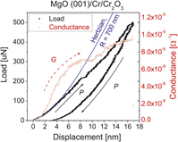
Thin native oxide layers can dominate the mechanical properties of metallic thin films. However, to date there has been little quantification of how such overlayers affect yield and fracture during indentation in constrained film systems. To gain insight into such processes, electrical contact resistance was measured in situ during nanoindentation on constrained thin films of epitaxial Cr and polycrystalline Al, both possessing a native oxide overlayer. Measurements during loading of the films show both increases and decreases in current, which can then be used to distinguish between various sources of plasticity. Ex situ measurements of the oxide thickness are used to provide a starting point for elasticity simulations of stress in both systems. The results show that dislocation nucleation in the metal film can be differentiated from oxide fracture during indentation.

Type
Articles
Copyright
Copyright © Materials Research Society 2012

Access options

Get access to the full version of this content by using one of the access options below. (Log in options will check for institutional or personal access. Content may require purchase if you do not have access.)

References

REFERENCES

1.Gane, N. and Bowden, F.P.: Microdeformation of solids. J. Appl. Phys. 39(3), 1432 (1968).CrossRefGoogle Scholar
2.Gerberich, W.W., Nelson, J.C., Lilleodden, E.T., Anderson, P., and Wyrobek, J.T.: Indentation induced dislocation nucleation: The initial yield point. Acta Mater. 44(9), 3585 (1995).CrossRefGoogle Scholar
3.Mann, A.B. and Pethica, J.B.: The role of atomic size asperities in the mechanical deformation of nanocontacts. Appl. Phys. Lett. 69(7), 907 (1996).CrossRefGoogle Scholar
4.Kramer, D., Huang, H., Kriese, M., Robach, J., Nelson, J., Wright, A., Bahr, D., and Gerberich, W.W.: Yield strength predictions from the plastic zone around nanocontacts. Acta Mater. 47(1), 333 (1999).CrossRefGoogle Scholar
5.Bahr, D.F., Kramer, D.E., and Gerberich, W.W.: Non-linear deformation mechanisms during nanoindentation. Acta Mater. 46(10), 3605 (1997).CrossRefGoogle Scholar
6.Kramer, D.E., Yoder, K.B., and Gerberich, W.W.: Surface constrained plasticity: Oxide rupture and the yield point process. Philos. Mag. A 81(8), 2033 (2000).CrossRefGoogle Scholar
7.Pethica, J.B. and Oliver, W.C.: Tip surface interactions in STM and AFM. Phys. Scr. T. 19, 61 (1987).CrossRefGoogle Scholar
8.Soer, W.A., Aifantis, K.E., and De Hosson, J.T.M.: Incipient plasticity during nanoindentation at grain boundaries in body-centered cubic materials. Acta Mater. 53, 4665 (2005).CrossRefGoogle Scholar
9.Ruffell, S., Bradby, J.E., Williams, J.S., and Warren, O.L.: An in situ electrical measurement technique via a conducting diamond tip for nanoindentation in silicon. J. Mater. Res. 22(3), 578 (2007).CrossRefGoogle Scholar
10.Nowak, R., Chrobak, D., Nagao, S., Vodnick, D., Berg, M., Tukiainen, A., and Pessa, M.: An electric current spike linked to nanoscale plasticity. Nat. Nanotechnol. 4, 287 (2009).CrossRefGoogle ScholarPubMed
11.Sharma, S.P. and Thomas, J.H.I.: Dielectric breakdown of Ag2S in the Au-Ag2S-Ag system. J. Appl. Phys. 47(5), 1808 (1975).CrossRefGoogle Scholar
12.Fang, L., Muhlstein, C.L., Collins, J.G., Romasco, A.L., and Friedman, L.H.: Continuous electrical in situ contact area measurement during instrumented indentation. J. Mater. Res. 23(9), 2480 (2008).CrossRefGoogle Scholar
13.Bhushan, B., Palacio, M., and Kinzig, B.: AFM-based nanotribological and electrical characterization of ultrathin wear-resistant ionic liquid films. J. Colloid Interface Sci. 317, 275 (2008).CrossRefGoogle ScholarPubMed
14.Pethica, J.B. and Tabor, D.: Contact of characterised metal surfaces at very low loads: Deformation and adhesion. Surf. Sci. 89, 182 (1979).CrossRefGoogle Scholar
15.Kim, D.I., Pradeep, N., DelRio, F.W., and Cook, R.F.: Mechanical and electrical coupling at metal-insulator-metal nanoscale contacts. Appl. Phys. Lett. 93, 203102 (2008).CrossRefGoogle Scholar
16.Maxwell, J.C.: Treatise on Electricity and Magnetism, Vol. 1, 3rd edition (Dover Publications, New York, NY, 1954).Google Scholar
17.Holm, R.: Electric Contacts. (Springer-Verlag, Berlin/Heidelberg/New York, 1967), pp. 155, 367–397.CrossRefGoogle Scholar
18.Greenwood, J.A. and Tripp, J.H.: The elastic contact of rough spheres. Trans. ASME, Series E. J. Appl. Mech. 34(153), 417 (1967).Google Scholar
19.Kogut, L. and Komvopoulos, K.: Electrical contact resistance theory for conductive rough surfaces. J. Appl. Phys. 94(5), 3153 (2003).CrossRefGoogle Scholar
20.Sharvin, Y.V.: On the possible method for studying fermi surfaces. Zh. Eksp. Teor. Fiz. 48, 984 (1965).Google Scholar
21.Nikolić, B. and Allen, P.B.: Electron transport through a circular constriction. Phys. Rev. B 60(6), 3963 (1998).CrossRefGoogle Scholar
22.Wexler, G.: The size effect and the non-local Boltzmann transport equation in orifice and disk geometry. Proc. Phys. Soc. 89, 927 (1966).CrossRefGoogle Scholar
23.Tholen, A., Erts, D., Olin, H., Ryen, L., and Olsson, E.: Maxwell and Sharvin conductance in gold point contacts investigated using TEM-STM. Phys. Rev. B 61(19), 12725 (2000).Google Scholar
24.Kogut, L. and Komvopoulos, K.: Electrical contact resistance theory for conductive rough surfaces separated by a thin insulating film. J. Appl. Phys. 95(2), 576 (2003).CrossRefGoogle Scholar
25.Matthiessen, A. and Vogt, C.: On the influence of temperature on the electric conductive-power of alloys. Philos. Trans. R Soc. London 154, 167 (1864).Google Scholar
26.Zuercher, R., Mueller, M., Sachslehner, F., Groeger, V., and Zehetbauer, M.: Dislocation resistivity in Cu: Dependence of the deviations from Matthiessen’s rule on temperature, dislocation density, and impurity content. J. Phys. Condens. Matter 7, 3515 (1995).CrossRefGoogle Scholar
27.Watts, B.R.: Calculation of electrical resistivity produced by dislocations in various metals. J. Phys. F: Met. Phys. 18, 1197 (1988).CrossRefGoogle Scholar
28.Sipos, B., Barisic, N., Gaal, R., Forro, L., Karpinski, J., and Rullier-Albenque, F.: Matthiessen’s rule in MgB2: Resistivity and Tc as a function of point defect concentration. Phys. Rev. B 76, 132504 (2007).CrossRefGoogle Scholar
29.Salomonsen, G., Norman, N., Lonsjo, O., and Finstad, T.G.: Kinetics and mechanism of oxide formation on titanium, vanadium, and chromium thin films. J. Less Common Met. 158, 251 (1990).CrossRefGoogle Scholar
30.Tamura, K., Kimura, Y., Suzuki, H., Kido, O., Sato, T., Tanigaki, T., Kurumada, M., Saito, Y., and Kaito, C.: Structure and thickness of natural oxide layer on ultrafine particle. Jpn. J. Appl. Phys. 42(12), 7489 (2003).CrossRefGoogle Scholar
31.Moodera, J.S., Gallagher, E.F., Robinson, K., and Nowak, J.: Optimum tunnel barrier in ferromagnetic-insulator-ferromagnetic tunneling structures. Appl. Phys. Lett. 70(22), 3050 (1997).CrossRefGoogle Scholar
32.Chia, R.W.J., Wang, C.C., and Lee, J.J.K.: Effect of adatom mobility and substrate finish on film morphology and porosity: Thin chromium film on hard disk. J. Magn. Magn. Mater. 209, 45 (2000).CrossRefGoogle Scholar
33.Parker, J., Wang, L., Steiner, K.A., Crowell, P.A., and Leighton, C.L.: Exchange bias as a probe of the incommensurate spin-density wave in epitaxial Fe/Cr (001). Phys. Rev. Lett. 97, 227206 (2006).CrossRefGoogle ScholarPubMed
34.Fitzsimmons, M.R. and Majkrzak, C.F.: Application of polarized neutron spectroscopy to studies of artificially structured magnetic materials. Modern Techniques for Characterizing Magnetic Materials, edited by Zhu, Y.. (Kluwer, Boston, 2005), pp. 107152.Google Scholar
35.Cheng, R., Borca, C.N., Xu, B., Yuan, L., Doudin, B., Liou, S.H., and Dowben, P.A.: Oxidation of metals at the chromium oxide interface. Appl. Phys. Lett. 81(11), 2109 (2002).CrossRefGoogle Scholar
36.Ikemoto, I., Kikujiro, I., Kinoshita, S., Kuroda, H., Alario Franco, M.A., and Thomas, J.M.: X-ray photoelectron spectroscopic studies of CrO2 and some related chromium compounds. J. Solid State Chem. 17(4), 425 (1976).CrossRefGoogle Scholar
37.Crist, B.V.: Handbook of Monochromatic XPS Spectra, Vol. 1, (XPS International, Inc., Mountain View, CA, 1999).Google Scholar
38.Castle, J.E., Chapman-Kpodo, H., Proctor, A., and Salvi, A.M.: Curve-fitting in XPS using extrinsic and intrinsic background structure. J. Electron. Spectrosc. Relat. Phenom. 106, 65 (2000).CrossRefGoogle Scholar
39.Aronniemi, M., Sainio, J., and Lahtinen, J.: Chemical state quantification of iron and chromium oxides using XPS: The effect of the background subtraction method. Surf. Sci. 578, 108 (2005).CrossRefGoogle Scholar
40.Fadley, C.S.: Instrumentation for surface studies: XPS angular distributions. J. Electron. Spectrosc. Relat. Phenom. 5(1), 725 (1974).CrossRefGoogle Scholar
41.Watts, J.F.: An Introduction to Surface Analysis by Electron Spectroscopy. (Oxford University Press, New York, NY, 1990), p. 7.Google Scholar
42.Seah, M.P. and Dench, W.A.: Quantitative electron spectroscopy of surfaces: A standard data base for electron inelastic mean free paths in solids. Surf. Interface Anal. 1(1), 2 (1979).CrossRefGoogle Scholar
43.Hertz, H.: On the contact of elastic solids. J. für reine angewandte Mechanik. Fur die reine und angewandte Mathematik. 92, 151 (1881) (An English translation is available as: Miscellaneous papers by H. Hertz, Eds Schott and Jones, MacMillan, London, 1896).Google Scholar
44.Johnson, K.L.: Contact Mechanics (Cambridge University Press, Cambridge, U.K., 1985), p. 90.CrossRefGoogle Scholar
45.Warren, O.L., Downs, S.A., and Wyrobek, T.J.: Challenges and interesting observations associated with feedback-controlled nanoindentation. Z. Metallkd. 95, 287 (2004).CrossRefGoogle Scholar
46.Villarrubia, J.S.: Algorithms for scanned probe microscope image simulation, surface reconstruction, and tip estimation. J. Res. Nat. Inst. Stand. Technol. 102, 425 (1997).CrossRefGoogle ScholarPubMed
47.Schwarzer, N.: FilmDoctor, SIO® (Saxonian Institute of Surface Mechanics,Ummanz, Germany, 2011), www.siomec.de.Google Scholar
48.Provenzano, V., Valiev, R., Rickerby, D.G., and Valdre, G.: Mechanical properties of nanostructured chromium. Nanostruct. Mater. 12, 1103 (1999).CrossRefGoogle Scholar
49.Firstov, S.A., Rogul, T.G., and Dub, S.N.: Grain boundary engineering of nanostructured chromium films, in Innovative Superhard Materials and Sustainable Coatings for Advanced Manufacturing, edited by Lee, J., Novikov, N., and Turkevich, V. (Springer, Netherlands, 2005) pp. 225232.CrossRefGoogle Scholar
50.Bobji, M.S., Biswas, S.K., and Pethica, J.B.: Effect of roughness on the measurement of nanohardness—a computer simulation study. Appl. Phys. Lett. 71(8), 1059 (1997).CrossRefGoogle Scholar
51.Gerberich, W.W., Tymiak, N.I., Grunlan, J.C., Horstemeyer, M.F., and Baskes, M.I.: Interpretations of indentation size effects. J. Appl. Mech. 69(4), 433 (2002).CrossRefGoogle Scholar
52.Habbab, H., Mellor, B.G., and Syngellakis, S.: Post-yield characterisation of metals with significant pile-up through spherical indentations. Acta Mater. 54(7), 1965 (2006).CrossRefGoogle Scholar
53.Saha, R. and Nix, W.D.: Effects of the substrate on the determination of thin film mechanical properties by nanoindentation. Acta Mater. 50(1), 23 (2002).CrossRefGoogle Scholar
54.Ohmura, T., Matsuoka, S., Tanaka, K., and Yoshida, T.: Nanoindentation load-displacement behavior of pure face centered cubic metal thin films on a hard substrate. Thin Solid Films 385(1-2), 198 (2001).CrossRefGoogle Scholar
55.Kramer, D.E., Volinsky, A.A., Moody, N.R., and Gerberich, W.W.: Substrate effects on indentation plastic zone development in thin soft films. J. Mater. Res. 16(11), 3150 (2001).CrossRefGoogle Scholar
56.Tsui, T.Y., Ross, C.A., and Pharr, G.M.: A method for making substrate-independent hardness measurements of soft metallic films on hard substrates by nanoindentation. J. Mater. Res. 18(6), 1383 (2003).CrossRefGoogle Scholar