Hostname: page-component-586b7cd67f-g8jcs Total loading time: 0 Render date: 2024-11-26T13:40:53.508Z Has data issue: false hasContentIssue false

On the root cause of Kirkendall voiding in Cu3Sn

Published online by Cambridge University Press:  04 February 2011

Liang Yin*
Affiliation:
Universal Instruments Corporation, Conklin, New York 13748
Peter Borgesen
Affiliation:
Department of Systems Science & Industrial Engineering, Binghamton University, Binghamton, New York 13902
*
a)Address all correspondence to this author. e-mail: [email protected]
Get access

Abstract

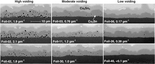
Soldering to Cu interconnect pads with Sn-containing alloys usually leads to the formation of a layered Cu3Sn/Cu6Sn5 structure on the pad/solder interface. Frequently, microscopic voids within Cu3Sn have been observed to develop during extended thermal aging. This phenomenon, commonly referred to as Kirkendall voiding, has been the subject of a number of studies and speculations but so far the root cause has remained unidentified. In the present work, 103 different Cu samples, consisting of 101 commercially electroplated Cu and two high-purity wrought Cu samples, were surveyed for voiding propensity. A high temperature anneal of the Cu samples before soldering was seen to significantly reduce the voiding level in subsequent thermal aging. For several void-prone Cu foils, the anneal led to significant pore formation inside the Cu. In the mean time, Cu grain growth in the void-prone foils showed impeded grain boundary mobility. Such behaviors suggested that the root cause for voiding is organic impurities incorporated in the Cu during electroplating, rather than the Kirkendall effect.

Type
Articles
Copyright
Copyright © Materials Research Society 2011

Access options

Get access to the full version of this content by using one of the access options below. (Log in options will check for institutional or personal access. Content may require purchase if you do not have access.)

References

REFERENCES

1.Shang, P.J., Liu, Z.Q., Li, D.X., and Shang, J.K.: Bi-induced voids at the Cu3Sn/Cu interface in eutectic SnBi/Cu solder joints. Scr. Mater. 58, 409 (2008).CrossRefGoogle Scholar
2.Shang, P.J., Liu, Z.Q., Pang, X.Y., Li, D.X., and Shang, J.K.: Growth mechanisms of Cu3Sn on polycrystalline and single crystalline Cu substrates. Acta Mater. 57, 4697 (2009).CrossRefGoogle Scholar
3.Chui, T., Zeng, K., Stierman, R., Edward, D., and Ano, K.: Effect of thermal aging on board level drop reliability for Pb-free BGA packages, in Proceedings of the 54th Electronic Component and Technology Conference (IEEE, NewYork, 2004), p. 1256.Google Scholar
4.Zeng, K., Stierman, R., Chui, T., Edward, D., Ano, K., and Tu, K.N.: Kirkendall void formation in eutectic SnPb solder joint on bare Cu and its effect on joint. J. Appl. Phys. 97, 024508 (2005).CrossRefGoogle Scholar
5.Mattila, T. and Kivilahti, J.: Reliability of lead-free interconnections under consecutive thermal and mechanical loadings. J. Electron. Mater. 35, 250 (2006).CrossRefGoogle Scholar
6.Xu, L., Pang, J., and Che, F.: Impact of thermal cycling on Sn-Ag-Cu solder joints and board-level reliability. J. Electron. Mater. 37, 880 (2008).CrossRefGoogle Scholar
7.Yu, J. and Kim, J.: Effects of residual S on Kirkendall void formation at Cu/Sn-3.5Ag solder joints. Acta Mater. 56, 5514 (2008).CrossRefGoogle Scholar
8.Anderson, I.E. and Harringa, J.L.: Elevated temperature aging of solder joints based on Sn-Ag-Cu: Effects on joint microstructure and shear strength. J. Electron. Mater. 33, 1485 (2004).CrossRefGoogle Scholar
9.Chao, B., Chae, S., Zhang, X., Lu, K., Ding, M., Im, J., and Ho, P.J.: Electromigration enhanced intermetallic growth and void formation in Pb-free solder joints. J. Appl. Phys. 100, 084909 (2006).CrossRefGoogle Scholar
10.Nah, J.W., Suh, J.O., and Tu, K.N.: Electromigration in flip chip solder joints having a thick Cu column bump and a shallow solder interconnect. J. Appl. Phys. 100, 123513 (2006).CrossRefGoogle Scholar
11.Liu, Y.C., Chen, J.T., Chuang, Y.C., Ke, L., and Wang, S.J.: Electromigration-induced Kirkendall voids at the Cu/Cu3Sn interface in flip-chip Cu/Sn/Cu joints. Appl. Phys. Lett. 90, 112114 (2007).CrossRefGoogle Scholar
12.Lai, Y.S., Chiu, Y.T., and Chen, J.: Electromigration reliability and morphologies of Cu pillar flip-chip solder joints with Cu substrate pad metallization. J. Electron. Mater. 37, 1624 (2008).CrossRefGoogle Scholar
13.Pieraggi, B., Rapp, R.A., van Loo, F.J.J., and Hirth, J.P.: Interfacial dynamics in diffusion-driven phase transformations. Acta Metall. Mater. 38, 1781 (1990).CrossRefGoogle Scholar
14.Yang, W., Messler, R.W., and Felton, L.E.: Microstructure evolution of eutectic Sn-Ag solder joints. J. Electron. Mater. 23, 250 (1994).CrossRefGoogle Scholar
15.Laurila, T., Vuorinen, V., and Kivilahti, J.K.: Interfacial reactions between lead-free solders and common base materials. Mater. Sci. Eng., R 49, 1 (2005).CrossRefGoogle Scholar
16.Liu, P.L. and Shang, J.K.: Segregant-induced cavitation of Sn/Cu reactive interface. Scr. Mater. 53, 631 (2005).CrossRefGoogle Scholar
17.Borgesen, P., Yin, L., Kondos, P., Henderson, D.W., Servis, G., Therriault, J., Wang, J., and Srihari, K.: Sporadic degradation in board level drop reliability—Those aren’t all Kirkendall voids!, in Proceedings of the 57th Electronic Component and Technology Conference (IEEE, NewYork, 2007), p. 136.Google Scholar
18.Wang, Y.W., Lin, Y.W., and Kao, C.R.: Kirkendall voids formation in the reaction between Ni-doped SnAg lead-free solders and different Cu substrates. Microelectron. Reliab. 49, 248 (2009).CrossRefGoogle Scholar
19.Kondos, P., Borgesen, P., and Yin, L.: Unpublished reports to AREA Consortium (2005).Google Scholar
20.Anderson, I.E. and Harringa, J.L.: Suppression of void coalescence in thermal aging of tin-silver-copper-X solder joints. J. Electron. Mater. 35, 94 (2006).CrossRefGoogle Scholar
21.Cho, M.G., Kang, S.K., Shih, D.Y., and Lee, H.M.: Effects of minor additions of Zn on interfacial reactions of Sn-Ag-Cu and Sn-Cu solders with various Cu substrates during thermal aging. J. Electron. Mater. 36, 1501 (2007).CrossRefGoogle Scholar
22.Wang, F., Yu, Z., and Qi, K.: Intermetallic compound formation at Sn-3.0Ag-0.5Cu-1.0Zn lead-free solder alloy/Cu interface during as-soldered and as-aged conditions. J. Alloys Compd. 438, 110 (2007).CrossRefGoogle Scholar
23.Ho, C., Yang, S., and Kao, C.: Interfacial reaction issues for lead-free electronic solders. J. Mater. Sci.—Mater. Electron. 18, 155 (2007).CrossRefGoogle Scholar
24.Gao, F., Nishikawa, H., and Takemoto, T.: Additive effect of Kirkendall void formation in Sn-3.5Ag solder joints on common substrates. J. Electron. Mater. 37, 45 (2008).CrossRefGoogle Scholar
25.Kim, J.Y., Yu, J., and Kim, S.H.: Effects of sulfide-forming element additions on the Kirkendall void formation and drop impact reliability of Cu/Sn–3.5Ag solder joints. Acta Mater. 57, 5001 (2009).CrossRefGoogle Scholar
26.Chu, J.P., Hsieh, Y.Y., Lin, C.H., and Mahalingam, T.: Thermal stability enhancement in nanostructured Cu films containing insoluble tungsten carbides for metallization. J. Mater. Res. 20, 1379 (2005).Google Scholar
27.Barmak, K., Gungo, A., Cabral, C., and Haper, J.M.E.: Annealing behavior of Cu and dilute Cu-alloy films: Precipitation, grain growth, and resistivity. J. Appl. Phys. 94, 1605 (2003).CrossRefGoogle Scholar
28.Borgesen, P., Yin, L., and Kondos, P.: Acceleration of the growth of Cu3Sn voids in solder joints. Microelectron. Reliab. (in press).Google Scholar
29.Oh, M.: Growth kinetics of intermetallic phases in the Cu-Sn binary and the Cu-Ni-Sn ternary systems at low temperatures. Ph.D. Thesis, Lehigh University, Bethlehem, PA, 1994.Google Scholar
30.Vuorinen, V., Laurila, T., Mattila, T., Heikinheimo, E., and Kivilahti, J.K.: Solid-state reaction between Cu(Ni) alloys and Sn. J. Electron. Mater. 36, 1355 (2007).CrossRefGoogle Scholar
31.Lide, D.R.: CRC Handbook for Chemistry and Physics, 84th ed. (CRC Press, Boca Raton, FL, 2003), pp. 12219.Google Scholar
32.Clark, F.: Advanced Techniques in Powder Metallurgy (Rowman and Littefield, New York, 1963), pp. 8087.Google Scholar
33.Thompson, C.V.: Grain growth in thin films. Annu. Rev. Mater. Sci. 20, 245 (1990).CrossRefGoogle Scholar
34.Merchant, H.D.: Defect structure of electrodeposits, in Defect Structure, Morphology and Properties of Deposits, edited by Merchant, H.D. (The Minerals, Metals and Materials Society, Warrendale, PA, 1995), p. 1.Google Scholar
35.German, R.M.: Powder Metallurgy Science, 2nd ed. (Metal Powder Industries Federation, Princeton, NJ 1994), p. 242.Google Scholar
36.Brongersma, S.H., Kerr, E., Vervoort, I., Saerens, A., and Maex, K.: Grain growth, stress, and impurities in electroplated copper. J. Mater. Res. 17, 582 (2002).CrossRefGoogle Scholar
37.Hau-Riege, S.P. and Thompson, C.V.: In situ TEM studies of the kinetics of abnormal grain growth in electroplated copper films. Appl. Phys. Lett. 76, 309 (2000).CrossRefGoogle Scholar
38.Liu, Y., Wang, J., Yin, L., Kondos, P., Parks, C., Borgesen, P., Henderson, D.W., Cotts, E.J., and Dimitrov, N.: Influence of plating parameters and solution chemistry on the voiding propensity at electroplated copper–solder interface. J. Appl. Electrochem. 38, 1695 (2008).CrossRefGoogle Scholar
39.Onishi, M. and Fujibuchi, H.: Reaction-diffusion in the Cu-Sn system. Tran. Jpn. Inst. Met. 16, 539 (1975).CrossRefGoogle Scholar
40.Paul, A.: The Kirkendall effect in solid state diffusion. Ph.D. Thesis, Eindhoven University of Technology, Eindhoven, The Netherlands, 2004, p. 82.Google Scholar
41.Henderson, D.W., Borgesen, P., Yin, L., and Kondos, P.: On the origins of “Kirkendall voiding” behavior in reactive interdiffusion couples. (In preparation).Google Scholar
42.Moffat, T.P., Wheeler, D., and Josell, D.: Electrodeposition of copper in the SPS-PEG-Cl additive system I. Kinetic measurements: Influence of SPS. J. Electrochem. Soc. 151, C262 (2004).CrossRefGoogle Scholar
43.Vereecken, P.M., Binstead, R.A., Deligianni, H., and Andricacos, P.C.: The chemistry of additives in damascene copper plating. IBM J. Res. Develop. 49, 3 (2005).CrossRefGoogle Scholar
44.Moffat, T.P., Wheeler, D., Edelstein, M.D., and Josell, D.: Superconformal film growth: Mechanism and quantification. IBM J. Res. Dev. 49, 19 (2005).CrossRefGoogle Scholar
45.Schultz, Z.D., Feng, Z., Biggin, M.E., and Gewirth, A.A.: Vibrational spectroscopic and mass spectrometric studies of the interaction of bis(3-sulfopropyl)-disulfide with Cu surfaces. J. Electrochem. Soc. 153, C97 (2006).CrossRefGoogle Scholar
46.Willey, M.J. and West, A.C.: SPS adsorption and desorption during copper electrodeposition and its impact on PEG adsorption. J. Electrochem. Soc. 154, C156 (2007).CrossRefGoogle Scholar
47.Tan, M., Guymon, C., Wheeler, D.R., and Harb, J.N.: The role of SPS, MPSA, and chloride in additive systems for copper electrodeposition. J. Electrochem. Soc. 154, D78 (2007).CrossRefGoogle Scholar
48.Wafula, F., Liu, Y., Yin, L., Bliznakov, S., Borgesen, P., Cotts, E.J., and Dimitrov, N.: Impact of key deposition parameters on the voiding sporadically occurring in solder joints with electroplated copper. J. Electrochem. Soc. 157, D111 (2009).CrossRefGoogle Scholar
49.Liu, Y., Yin, L., Bliznakov, S., Kondos, P., Borgesen, P., Henderson, D.W., Parks, C., Wang, J., Cotts, E.J., and Dimitrov, N.: Improving copper electrodeposition in the microelectronics industry. IEEE Trans. Compon. Packag. Technol. 33, 127 (2010).CrossRefGoogle Scholar
50.Yin, L., Dimitrov, N., and Borgesen, P.: Kirkendall voiding and impurity incorporation in Cu electroplating. (In preparation).Google Scholar